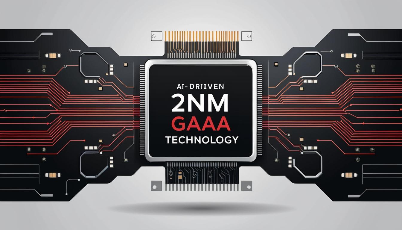
A strategic collaboration between Synopsys and Rapidus aims to revolutionise the semiconductor design process by introducing advanced techniques that utilise artificial intelligence (AI) automation. This partnership focuses on enhancing design flows and optimising manufacturing processes, particularly around Rapidus' innovative 2nm gate-all-around (GAA) technology.
The two companies have announced that they are “using a revolutionary new approach to natively model process sensitivity and variation in the design steps.” This approach is expected to “dramatically reduce the need for expensive re-characterisation of libraries and memories during different phases of the process evolution leading to a significant reduction in design iterations and acceleration of the overall project execution cycle.”
Characterisation of the intellectual property (IP) library is often cited as a significant bottleneck in the semiconductor design cycle, mainly due to the need for re-characterisation whenever there are updates to the process design kit (PDK) or manufacturing processes. Traditionally, this re-characterisation may take two to three months, considerably slowing down design timelines. To address this, Synopsys' AI-driven electronic design automation (EDA) suite will be employed, including the Synopsys PrimeShieldTM — a machine learning-based timing model generation tool that harnesses sensitivity libraries to expedite and enhance accuracy in model generation.
Sassine Ghazi, president and CEO of Synopsys, highlighted the importance of this collaboration by stating, “Synopsys continues to play a mission-critical role as an on-ramp to the world’s leading foundries and we are often the first stop for foundry enablement.” He emphasised that the extensive collaboration would facilitate the advanced Design for Manufacturing and Co-Optimization (DMCO) concept, enabling simultaneous optimisation of design and manufacturing processes.
This new approach extends beyond mere design adjustments; Rapidus is integrating the concept of Manufacturing for Design (MFD) alongside traditional Design for Manufacturing (DFM). By using sensors and AI in their wafer processes, Rapidus will streamline design optimisation based on extensive silicon data gathered during manufacturing. This integration of big data with Synopsys EDA flows is anticipated to reduce integration risks and speed up the transition from design to actual silicon production.
Dr. Atsuyoshi Koike, CEO of Rapidus, described the partnership as an important milestone that simplifies and accelerates the design process. He noted, “Our partnership with Synopsys is an important milestone in helping to simplify and quicken the design process. Rapidus’ vision for RUMS is to use a single-wafer front-end process. The massive amount of data that can be obtained from this process is highly compatible with Synopsys AI-driven EDA flows and IP, and we believe that this will be a step toward achieving our goal of short turnaround time (TAT) production that is quicker than anywhere else.”
In addition to the collaboration with Synopsys, Rapidus has also announced a partnership with Cadence to provide co-optimised AI-driven reference design flows and a comprehensive IP portfolio to support their 2nm GAA process and backside power delivery network (BSPDN) technology. This dual approach reinforces a concerted effort to push the boundaries in semiconductor design, focusing on improving efficiency and reducing time-to-market for new products.
Source: Noah Wire Services