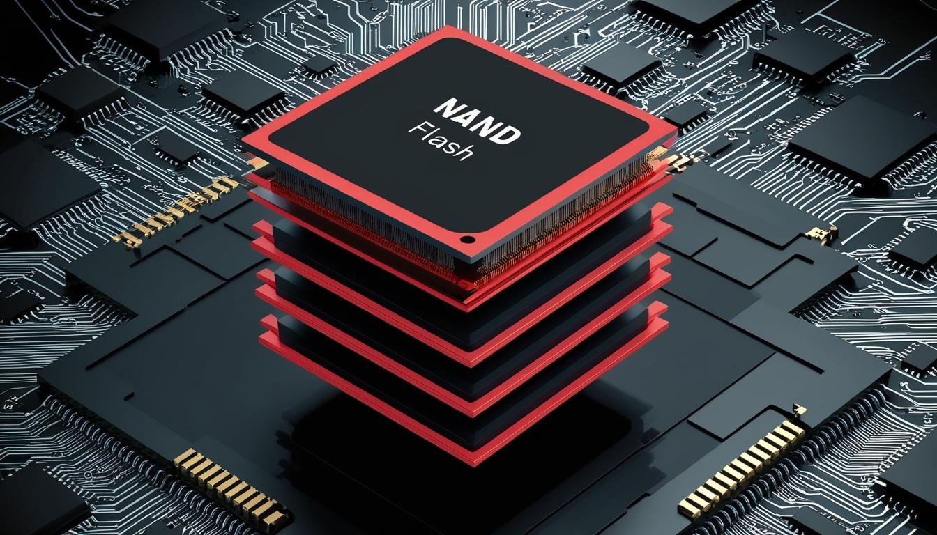
In a significant advancement within the technology sector, SK Hynix has announced the mass production of a groundbreaking 321-layer NAND flash memory, specifically designed to cater to the demands of artificial intelligence (AI) and high-capacity data storage. This new 1-terabit triple-level cell (TLC) 4D NAND flash memory, unveiled recently, positions SK Hynix at the forefront of the NAND flash memory market, as they are the first to exceed 300 layers.
The launch of the 321-layer NAND comes as a response to the increasing needs of AI-driven applications, which require efficient, high-performance storage solutions. Set to be supplied to customers in the first half of 2025, this new technology is anticipated to revolutionise the industry by enabling the production of ultra-high-capacity solid-state drives (SSDs) that can surpass 100TB.
The achievement is a continuation of SK Hynix's innovations, following the successful introduction of their 238-layer NAND flash last year. This new development not only elevates the industry standard but also reflects the intense competition in the market, particularly between SK Hynix and its main rival, Samsung. The capabilities of the 321-layer NAND are underscored by a 12% improvement in data transfer speed, a 13% enhancement in reading performance compared to the previous model, and a reduction in power consumption exceeding 10%.
The technological prowess behind the 321-layer NAND resides in SK Hynix's proprietary "Three Plugs" process technology. This method enables the electrical connection of three plugs through a meticulously optimised procedure, enhancing speed, power efficiency, and overall chip performance. Furthermore, the development of low-stress materials and alignment-correcting technology optimises the manufacturing process, significantly boosting productivity by 59%.
Industry experts anticipate that this wave of innovation will not cease with SK Hynix. Samsung is reportedly in active development of its own 400-layer NAND flash chip, projected for release by 2026. With a roadmap that includes bonding vertical NAND (BV NAND) technology, Samsung aims for enhanced storage density and reduction in heat output. Their long-term aspirations encompass the creation of NAND chips exceeding 1,000 layers by the year 2030, which could potentially breach the 200TB storage threshold for SSDs designed for AI applications.
Jungdal Choi, Head of NAND Development at SK Hynix, commented on the company's direction, stating, "SK Hynix is on track to advancing to the Full Stack AI Memory Provider by adding a perfect portfolio in the ultra-high performance NAND space on top of the DRAM business led by HBM."
As the landscape of data storage continues to evolve, the rivalry between these two tech giants promises to drive further innovations, catering to the escalating requirements of AI technologies and other data-intensive applications.
Source: Noah Wire Services