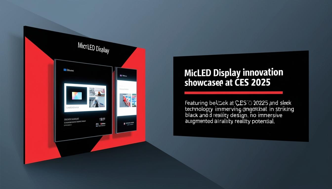
At CES 2025, Aledia has launched its innovative microLED technology, poised to revolutionise the hardware landscape for augmented reality (AR) and vision applications. This announcement marks a significant milestone in the development of smart displays, particularly as tech giants pivot towards microLED solutions for smart glasses, aiming for prototypes to transition into commercial products by 2027.
The introduction of AI-powered applications in AR over the past year underscored the growing interest in the sector; however, challenges such as power consumption, bulkiness, and high manufacturing costs have historically hindered widespread adoption. After 12 years of dedicated research and development, which accumulated to nearly 300 patents and over $600 million in investment, Aledia asserts it has overcome these obstacles with its microLED-based microdisplay technology, which promises enhanced efficiency and performance.
Pierre Laboisse, the president and CEO of Aledia, emphasised the need for advanced display technologies, stating, “Immersive technologies such as AR haven’t reached their full potential as the industry has yet to design screens that are both slick and highly functional.” He elaborated on Aledia’s advancements, saying, “At Aledia, we’ve created a nanowire technology that makes microLED displays thinner, more power efficient and easier to produce for mass adoption.” Laboisse also forecasted a shift in the market, claiming, “By next CES, OLED and LCOS will already be phased out in favor of our superior microLED technology.”
The microLED system developed by Aledia is distinguished by its use of 3D gallium nitride (GaN) grown on silicon nanowires, which enhances both brightness and energy efficiency compared to traditional 2D LED technology. The 3D design facilitates precise and directive light emission, key for facilitating immersive AR experiences. In testing phases, Aledia's nanowires showed significant improvements in light directivity and efficiency, essential features for advanced display applications.
Moreover, the company's hybrid bonding technology allows for the integration of microLEDs and driver electronics into compact chips, significantly improving power efficiency and extending battery life in thinner displays. Aledia’s commitment to scaling production is underpinned by its over $200 million pilot production line located in the heart of Europe’s “Display Valley.” This facility enables rapid iteration and lowers production costs for large-scale microLED production, positioning Aledia to meet an anticipated ramp-up in customer demand of up to 5,000 wafer starts weekly.
Laboisse highlighted the significance of Aledia’s facilities, remarking, “Our Champagnier factory is a key milestone for European innovation, and we are proud to represent it at the Auvergne Rhône-Alpes Pavilion at CES.” He concluded with a vision for the future, asserting that Aledia is redefining global display technology standards and positioning Grenoble as a hub for microLED manufacturing.
Those interested in Aledia’s innovative technology can visit Booth 60711-04 at Eureka Park in Hall G at the Venetian during CES 2025. The company is also facilitating exclusive interviews with its executives and private meetings at the Venetian Resort for interested parties.
Source: Noah Wire Services