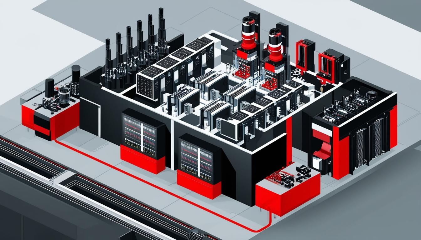
The semiconductor industry is poised for significant growth, with projections indicating the commencement of 18 new fabrication facility construction projects in 2025. This forecast, detailed in SEMI’s latest quarterly World Fab Forecast report, reveals a strategic expansion in response to escalating global demands for both leading-edge and mainstream semiconductor technologies.
Among the new projects, the breakdown includes three facilities dedicated to 200mm wafers and fifteen focused on 300mm wafers, the majority of which are expected to become operational between 2026 and 2027. Regions such as the Americas and Japan are at the forefront, both planning four projects each, while China and Europe & the Middle East follow closely with three projects apiece. Taiwan has announced two projects, and both Korea and Southeast Asia are preparing for one project each in the same year.
Ajit Manocha, president and CEO of SEMI, articulated the industry’s trajectory, stating, “The semiconductor industry has reached a pivotal juncture, with investments driving both leading-edge and mainstream technologies to meet evolving global demands.” He highlighted that advancements in generative AI and high-performance computing (HPC) are vital drivers for progress in the leading-edge logic and memory segments. According to Manocha, the establishment of these 18 new semiconductor fabs illustrates the industry's commitment to innovation and economic growth.
The World Fab Forecast report, which covers the period from 2023 to 2025, outlines a broader context wherein the global semiconductor sector anticipates the initiation of 97 new high-volume fabs. The report indicates that 48 of these projects are set to kick off in 2024, followed by 32 in 2025, utilising wafer sizes that range from 300mm to 50mm.
In terms of production capacity, the semiconductor industry is projected to witness a 6.6 percent annual growth rate, scaling up to a total capacity of 33.6 million wafers per month by 2025. This augmentation is primarily attributed to advancements in leading-edge logic technologies for HPC applications, alongside an increasing incorporation of generative AI into edge devices. Chip manufacturers appear to be focusing on bolstering capacities at advanced node levels (7nm and below), with an expected growth rate of 16 percent annually, resulting in a surge of over 300,000 wafpm to reach a total of 2.2 million wafpm in 2025.
The report also outlines how China's strategy for chip self-sufficiency, coupled with rising demands from automotive and Internet of Things (IoT) applications, is expected to amplify capacity in mainstream nodes (8nm to 45nm), projecting a 6 percent increase and surpassing the milestone of 15 million wafpm in 2025. In contrast, the mature technology nodes (50nm and above) are anticipated to grow at a more conservative rate of 5 percent, culminating in a total of 14 million wafpm by 2025, reflective of a slow market recovery and lower utilisation rates.
Foundry suppliers are anticipated to continue leading in semiconductor equipment investments, with the foundry segment expected to expand capacity by 10.9 percent year-on-year, reaching a record high of 12.6 million wafpm in 2025, up from 11.3 million wafpm in 2024. Meanwhile, the memory segment is forecasted to experience slow but steady growth; specifically, the DRAM segment is projected to grow by approximately 7 percent year-over-year to reach an installed capacity of 4.5 million wafpm in 2025, while the NAND flash segment is expected to experience a 5 percent rise, reaching 3.7 million wafpm by the same period.
The latest SEMI World Fab Forecast report, updated in December 2024, includes a comprehensive list of over 1,500 semiconductor facilities and lines globally, with 180 volume facilities anticipated to start operations in 2025 or later.
Source: Noah Wire Services