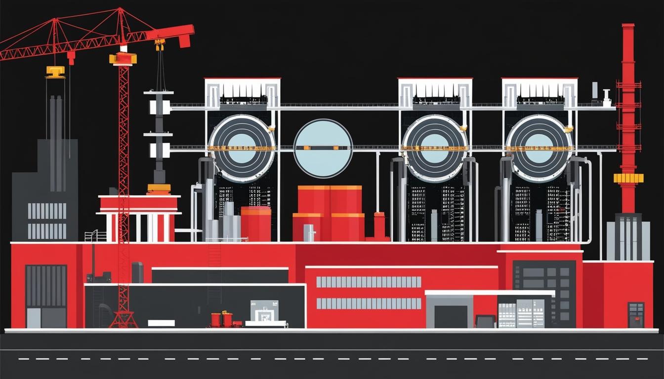
The semiconductor industry is gearing up for a significant expansion, with plans to initiate the construction of 18 new fabrication facilities (fabs) in 2025, as detailed in SEMI's latest quarterly World Fab Forecast report. This strategic move is indicative of the increasing demands for both advanced and mainstream technology applications, with the new fabs set to include three 200mm and fifteen 300mm facilities. Operations for the majority of these projects are anticipated to commence between 2026 and 2027.
According to the report, the Americas and Japan will lead the charge with four projects each in 2025, while China and the Europe & Middle East regions are each set to initiate three construction projects. Taiwan follows with two, and both Korea and Southeast Asia contribute one project each to the forecast. "The semiconductor industry has reached a pivotal juncture, with investments driving both leading-edge and mainstream technologies to meet evolving global demands," remarked Ajit Manocha, SEMI President and CEO. Speaking to Semiconductor Digest, he further stated, “Generative AI and high-performance computing are fueling advancements in the leading-edge logic and memory segments, while mainstream nodes continue to underpin critical applications in automotive, IoT and power electronics."
The World Fab Forecast report highlights that from 2023 to 2025, the global semiconductor sector is poised to launch an impressive total of 97 new high-volume fabs, with 48 projects expected to go live in 2024 followed by an additional 32 in 2025. The wafer_sizes are diverse, ranging from 300mm down to 50mm.
Capacity growth in the semiconductor industry is on a steady upward trend, projected to achieve a 6.6% annual growth rate, culminating in a total production capacity of 33.6 million wafers per month (wpm) by 2025. This growth is largely attributed to advancements in leading-edge logic technologies, particularly in high-performance computing (HPC), as well as the increasing use of generative AI in edge devices.
The report indicates a robust investment in advanced node capacities, specifically in nodes of 7nm and below, which are expected to see an exceptional growth rate of 16%, adding over 300,000 wpm to reach a total of 2.2 million wpm by 2025. Meanwhile, mainstream technology nodes, classified as ranging from 8nm to 45nm, are projected to experience a 6% capacity increase, exceeding the milestone of 15 million wpm in the same timeframe. The more mature technology nodes, defined as 50nm and above, are likely to expand at a slower rate of 5%, achieving 14 million wpm by 2025 due to a gradual market recovery and diminished utilization rates.
The foundry segment is anticipated to take a leading role in semiconductor equipment procurement, with a projection that it will bolster capacity by 10.9% year-over-year, climbing from 11.3 million wpm in 2024 to a record 12.6 million wpm in 2025. In contrast, the overall memory segment is set to witness more modest capacity growth, with an anticipated increase of 3.5% in 2024 and 2.9% in 2025.
The driving force behind some of these changes in the memory market is the heightened demand stemming from generative AI applications. The high-bandwidth memory (HBM) sector is notably experiencing significant growth. Within the memory landscape, DRAM is projected to flourish with a 7% year-on-year increase, reaching approximately 4.5 million wpm in 2025, while the 3D NAND segment is expected to add 5% capacity, achieving 3.7 million wpm during the same period.
The SEMI World Fab Forecast report, which provided this comprehensive overview, unveiled details regarding over 1,500 semiconductor facilities and production lines globally, which includes 180 volume facilities and lines with scheduled operations expected to start in 2025 or later. This robust outlook for the semiconductor industry reflects ongoing investments, supported by innovations in technology that aim to meet the growing demands of a wide array of sectors.
Source: Noah Wire Services