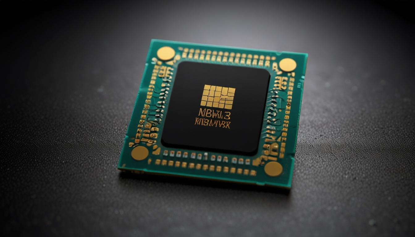
SK Hynix Commences Mass Production of Revolutionary 12-Layer HBM3E Memory
Seoul, South Korea – SK Hynix, a leader in the semiconductor industry, has announced the commencement of mass production of its pioneering 12-layer High Bandwidth Memory 3 Enhanced (HBM3E). This development marks a significant stride in memory technology, pushing the boundaries of performance and capacity.
The new HBM3E offers an unprecedented 36GB total memory capacity, eclipsing the previous generation's 24GB offered in an 8-layer configuration. This advancement has been made possible by a remarkable reduction in the thickness of each DRAM chip by 40%, enabling more layers to be stacked without increasing the overall size of the memory module.
Planned to begin volume shipments by the end of 2024, the HBM3E memory features a bandwidth of 9600 Mega-transfers per second (MT/s). In an eight-stack configuration, this bandwidth equates to an effective data transfer speed of 1.22 terabytes per second (TB/s). Such capabilities render it particularly suitable for large language models (LLMs) and artificial intelligence (AI) workloads that demand both high capacity and rapid data processing speeds. The increased efficiency can significantly enhance the running of AI models by facilitating quicker data computation.
SK Hynix has employed cutting-edge packaging technologies in this advanced memory stacking process. The Through Silicon Via (TSV) and Mass Reflow Molded Underfill (MR-MUF) processes play critical roles in ensuring the structural integrity and effective heat dissipation necessary for the stable operation of the HBM3E. Enhancements in heat dissipation are vital for maintaining reliability during demanding AI processes, which can generate considerable heat.
Enhanced stability is another hallmark of the HBM3E, with SK Hynix’s proprietary packaging processes ensuring reduced warpage during the stacking process. The company’s MR-MUF technology is designed to manage internal pressure effectively, minimising the risks of mechanical failures and ensuring robust long-term durability.
Initial samples of the 12-layer HBM3E were available as early as March 2024. Notable among the next-generation hardware expected to integrate this cutting-edge memory are Nvidia’s Blackwell Ultra GPUs and AMD’s Instinct MI325X accelerators. These products are anticipated to leverage up to 288GB of HBM3E, catering to complex AI computations and innovations.
SK Hynix has prioritised the provision of its HBM3E to Nvidia, declining a $374 million advanced payment from an undisclosed entity to ensure an adequate supply for Nvidia's highly sought-after AI hardware.
Justin Kim, President and Head of AI Infrastructure at SK Hynix, emphasised the company's leadership in AI memory technology. "SK Hynix has once again broken through technological limits, demonstrating our industry leadership in AI memory," he remarked. "We will continue our position as the No.1 global AI memory provider as we steadily prepare next-generation memory products to overcome the challenges of the AI era."
The introduction of HBM3E into the market underscores SK Hynix’s commitment to advancing memory technology in alignment with the evolving demands of AI and data processing industries. The company's innovative approach continues to make significant impacts on the capabilities of modern computing technologies.
Source: Noah Wire Services