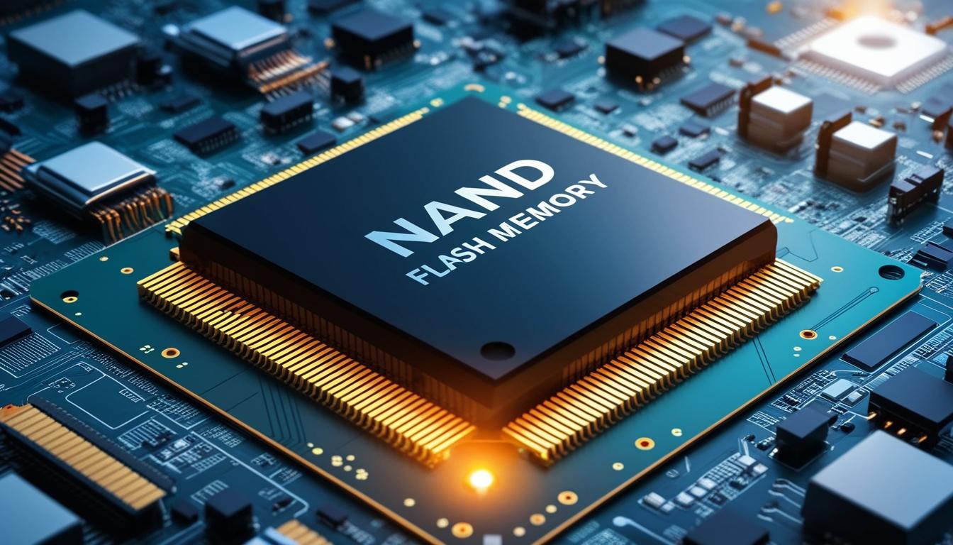
The landscape of electronics is undergoing a significant transformation as innovations in NAND flash memory continue to evolve. NAND, a critical component that drives storage capacity, performance, and power efficiency, is integral to diverse electronic devices and systems, from data center servers to personal gadgets like mobile phones, drones, and cameras. As these devices integrate more advanced features and undertake complex tasks, particularly in artificial intelligence (AI), the demand for substantial data storage solutions is more pressing than ever.
In the quest to cater to this burgeoning demand, the focus has shifted from merely increasing the number of NAND layers to exploring multifaceted innovations to enhance NAND memory. Traditionally, increasing the vertical layer count of NAND was seen as the primary method to boost bit density and storage capacity, envisaged as a linear path toward cost efficiency. However, experts like Dr. Luca Fasoli, Senior Vice President of Development Engineering at Western Digital, argue that this approach parallels adding floors to a hotel, where each addition incurs escalating costs and complexity.
Instead, the current evolution in NAND technology is marked by strategic innovations across various scaling methods: lateral, logical, and architectural, in addition to traditional vertical scaling. Lateral scaling, for instance, enhances each existing memory layer's efficiency by optimizing available space, akin to maximizing room occupancy on a hotel floor by minimizing redundant spatial elements. This method not only saves costs but also attracts reduced risks associated with over-layered structures.
Simultaneously, logical scaling focuses on increasing the logical storage capacity within a single physical unit, similar to accommodating more guests in a hotel room without disruption. Architecture scaling involves reconfiguring circuit positions adjacent to or integrated with memory arrays, comparable to strategically placing essential services like parking around a hotel.
These diversified approaches represent a paradigm shift in NAND development, moving away from a one-dimensional layer-focused strategy to a more nuanced model that leverages the strengths of each method. By applying a combination of these scaling vectors, NAND flash memory can achieve greater bit growth, maintain superior performance and power efficiency, and offer tailored solutions across a wide range of applications and devices.
This transformative phase in NAND technology is particularly relevant as new applications—especially those related to AI—demand increasingly sophisticated, compute- and storage-intensive flash solutions. The AI Data Cycle framework exemplifies this demand, where storage both fuels AI model training and is subsequently driven to expand further by AI's resource requirements. Consequently, this interaction is anticipated to be a major growth catalyst for the storage industry.
During NAND nodal migrations, the focus has also shifted to responding to the specific needs of diverse customers rather than adhering to a uniform approach. Different devices require distinct storage solutions, and what customers aim to build now determines how the storage should function—size, capacity, and power consumption are all dictated by the customer's ultimate goal. Accordingly, this customer-centric approach mitigates the traditional emphasis on simply multiplying layers and instead prioritizes essential performance attributes like speed, power efficiency, and capacity.
As these developments unfold, NAND flash memory remains at the forefront of electronic innovations, reshaping how data is stored, processed, and utilised across technological landscapes. This ongoing evolution reflects a responsive and strategic industry adaptation designed to meet the emerging needs of modern technology applications.
Source: Noah Wire Services