Artificial intelligence (AI) is rapidly transforming multiple sectors, leading to significant advancements in semiconductor technology, particularly in silicon fabrication. As reported by In Compliance Magazine, the surge in AI's application has resulted in increased manufacturing of high bandwidth memory (HBM) stacks, which play a critical role in enhancing the efficiency and speed of data transfer in electronic devices powered by AI algorithms.
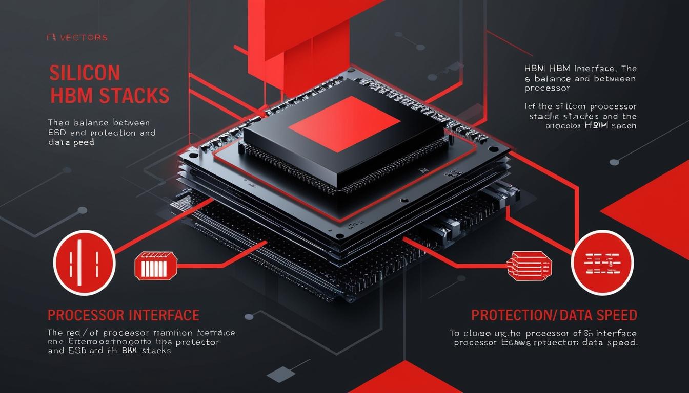
The development of HBM stacks, situated close to processors, marks a pivotal improvement in memory density, significantly boosting the performance of devices. However, the complexities in creating multiple die stacks introduce concerns regarding electrostatic discharge (ESD) at the die-to-die (D2D) interface during production. As stated in the report, "there is a requirement to balance the amount of ESD protection on the interface without interfering with the speed, silicon area, and design at the interface." This balance is becoming increasingly complex as the advances in D2D interconnects result in smaller and denser configurations, further constraining the acceptable thresholds for ESD protection.
To address these challenges, the ESD industry council has recently updated a white paper that delineates the charge device model (CDM) specifications and requirements specifically tailored for D2D interfaces. The document provides a roadmap for aligning manufacturing ESD levels with the necessary ESD protections, reflecting the future reduction in CDM targets as D2D interface densities continue to escalate.
Moreover, the report highlights the risk of cumulative ESD damage due to an increase in die stacks. It indicates that multiple stacks can lead to repetitive ESD events, which could propagate through the die interconnect with every layer added. Figures presented in the white paper illustrate that even within the “acceptable” D2D voltages, such stress can result in oxide degradation and affect the time-to-fail metrics associated with ESD events.
A tool known as the very-fast transmission line pulse (vfTLP) has been identified as critical for evaluating on-chip ESD design elements. The tool can simulate increased stress levels from rapid pulses to observe the cumulative effects on device integrity. Measured data indicates a decline in performance across gate oxide layers and diminished fusing capabilities within metal interconnects as a result of these cumulative stresses.
In summary, the advancements in silicon fabrication linked to AI demand a careful calibration between necessary protection from ESD and the need to maintain operational efficiency and size limitations. The updated white paper from the ESD council is designed to assist in achieving this equilibrium, yet it highlights that innovative developments in D2D interfaces may introduce unique considerations that warrant further investigation and adaptation.
Source: Noah Wire Services