Imec, a leading research hub in nanoelectronics and digital technologies, is charting the future of CMOS technology through a focus on innovations that extend beyond Moore's Law and the dimensions of traditional semiconductor scaling. César Javier Lockhart de la Rosa, Program Manager Exploratory Logic at imec, and Gouri Sankar Kar, Vice President of Compute & Memory Device Technologies at imec, have shared insights into how the semiconductor industry is navigating a landscape where purely dimensional scaling is no longer sufficient for enhancing chip performance.
This shift became apparent around 2005, when the anticipated performance improvements driven by Dennard scaling began to wane. Industry experts have recognised that to maintain the advantages of performance, power efficiency, area, and cost, it is essential to combine lithography advancements with new technology innovations at various levels, including material and architectural developments at the transistor level.
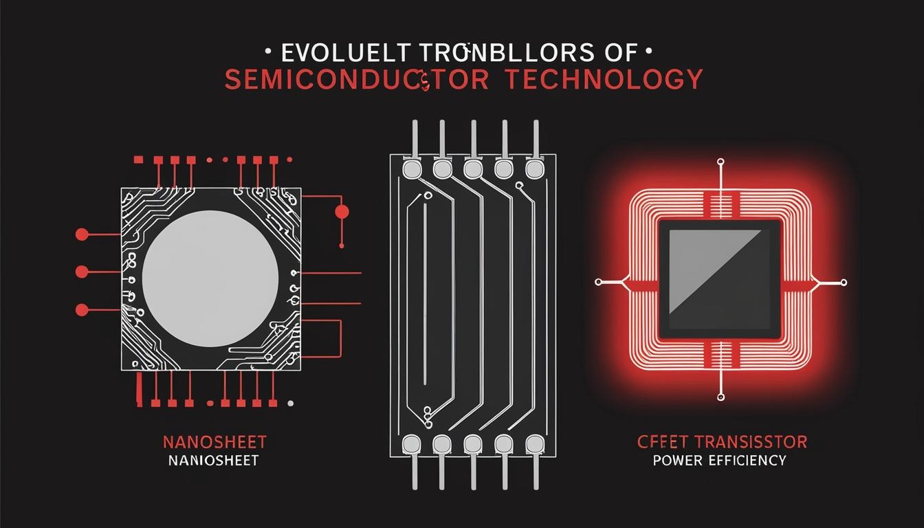
The evolution in chip design has seen the industry transition from planar MOSFET technology to more advanced structures such as FinFETs, and now gate-all-around (GAA) nanosheet transistors. These innovations allow for improved electrostatic control over the conduction channel, essential for high-performance computing applications. According to Lockhart de la Rosa, the introduction of nanosheet transistors is expected to sustain the logic scaling roadmap across three additional technology generations when paired with advances at the standard cell level.
In the perspective of imec, one of the groundbreaking innovations on the horizon is the complementary FET (CFET) which is set to enable greater integration efficiency by vertically stacking n-type and p-type channels. The anticipated introduction of CFETs starting from the A7 technology node will extend the technology roadmap to the A3 generation. The design features of CFETs ensure complete electrostatic control, as the gate fully enwraps both silicon channels.
However, as advancements unfold towards even smaller transistors, challenges persist. The continuing trend of reducing gate and channel lengths raises concerns about performance degradation due to short channel effects. To tackle this issue, imec is looking towards the integration of two-dimensional (2D) materials, specifically transition metal dichalcogenides (MX2), which possess a unique atomic structure conducive to thin channel designs. These materials not only enable the construction of channels thinner than 10nm but also promise to maintain significant carrier mobility.
Despite the potential advantages offered by 2D semiconductors, their integration into existing technologies comes with considerable challenges, as outlined by Kar. The introduction of 2D materials into advanced transistor nodes could increase costs and complicate the integration efforts required to successfully implement the A2 node.
The current direction of research suggests that with continued investment from major chip manufacturers and research institutions, the semiconductor industry is poised to overcome the barriers presented by 2D material integration. This pursuit is critical as the demand for smaller, faster, and more efficient electronic devices grows, setting the stage for next-generation semiconductor technologies.
Key developments in materials science and transistor architecture remain central to the narrative of semiconductor evolution, marking a significant chapter in the transformation of business practices across numerous industries reliant on advanced computing technologies.
Source: Noah Wire Services